PERIPHERALS
Peripherals (of a processor) are its means of communicating with the external world.
(1) Peripheral Classification
Peripherals can be classified based on following characteristics
Simplex, Duplex & Semi DuplexSimplex communication involves unidirectional data transfers. Duplex communication involves bi-directional data transfers. Full Duplex interfaces have independent channels for transmission and reception. Semi-duplex communication involves data bi-directional data transfers, however at a given time, the data transfer is only possible in one direction. Semi-duplex interfaces involves the same communication channel for both transmission and reception.
Serial Vs ParallelSerial peripherals communicate over a single data line. The data at Tx end needs to be converted “Parallel to Serial” before transmission and the data at Rx end needs to be converted “Serial to Parallel” after reception. Serial peripherals imply less signal lines on the external interface and thus reduced hardware (circuit board) complexity and cost. However the data rate on serial interfaces are fairly limited (as compared to the parallel interface). At the same clock rate, parallel interface can transfer Nx data, as compared to the serial interface (where N is the number of Data lines).
Synchronous Vs AsynchronousSynchronous transfers are synchronized by a reference clock on the interface. This clock signal is generally provided by one of the devices (who are communicating) on the interface, called master device. However clock can also come from an external source.
Data ThroughputInterfaces can also be classified based on the data throughput they offers. Generally parallel interfaces provide much more data throughput and are used for application data (this data needs to be processed by the application). Serial interfaces offer less data throughputs, and are generally used to transfer intermittent control data.
(2) Common Serial Peripherals
(a) UART (Universal Asynchronous Receiver Transmitter)
UART is one of the oldest and most simple serial interface. Generally UART is used to tranfer data between different PCBs (Printed Circuit Boards). These PCBs can be either in the same system or across differnt systems. In its simplest configuration, UART consists of two pin interface. One pin is used for Transmission, and other for Reception.
The data on UART is transferred word by word. A word consists of Start Bit, Data bits (5 to 8), (and optional parity bit) and (1, 1.5 or 2) Stop Bit. The individual bits of data word are transferred one by one on the serial bus.
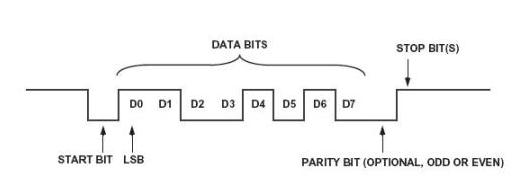
Start Bit: The Tx Line of a UART Transitter is high during periods of inactivity (when no communication is taking place). When the transmitter wants to initiate a data transmission it sends one START bit (drives the Tx line low) for one bit duration.
Data Bits: Number of data bits can be configured to any value between 5 and 8. UART employs LSB first Transmission.
Parity Bit: One parity bit can be optionally transitted along with each data word. The parity bit can be configured either as Odd or as even.
Stop Bit: After each word transmission, transmitter transmits Stop bits (drives the Tx line high). Number of stop bits can be configured as 1, 1.5 or 2.
Asynchronous Transmission: UART data transfers are asynchronous. The transmitter transmits each bit (of the word being transmitted) for a fixed duration (defined by baud rate). The receiver polls the value of transmit line (of transmitter). In order to be able to receive the data correctly, receiver needs to be aware of the duration for which each bit is transmitted (it is defined by baud rate).
Baud Rate: Baud is a measurement of transmission speed in asynchronous communication. It is defined as the number of distinct symbol changes made to the transmission media per second. Since UART signal has only two levels (high and low), baud rate here is also equal to the bit rate.
RS-232 and DB-9
UART can be used to transfer data directly across any two devices. However the most common usage of UART involves transfer of data from a PC (or other host computer) to a remote board (other slave device). Under such scenarios (where distance between two devices is more than a few inches), physical interface between Tx and Rx devices is defined by RS-232 specifications. Signals at each end are terminated to a 9-pin (DB-9) connector.
Debugging UART Interface
Following steps could be helpful while debugging communication problems on a UART interface
(a) UART loop-back: Run the internal loop-back tests on both Rx and Tx (most UART devices provide this functionality). This will ensure that each device is functional (not damaged)
(b) Check the Configuration: If the communication between two devices is failing, there could be a configuration mismatch between Tx and Rx. Cross-check the configuration at both sides and ensure that it is identical.
(c) Check the Serial Cable: Generally two UARTs are connected through a serial cable (which has 9-pin connectors on both sides). The cable should be a cross-over (Tx on one side connects to Rx on other side). A faulty (damaged or wrong corssings) serial cable can also cause erratic behavior. Make sure that cable is not damaged.
(d) Probe the Tx signal: If UART communication still remains erratic (after checks a, b and c), the last resort would be to probe the UART signals using a scope.
Limitation: Both the sender and receive should agree to a predefined configuration (Baud Rate, Parity Settings, number of data and stop bits). A mismatch in the configuration at two ends (Transmitter and Receiver), will cause communication failure (data corruption). Data rates are very slow. Also, if there are more devices involved in communication, the number of external pins needed on the device increase proportionally.
(b) SPI
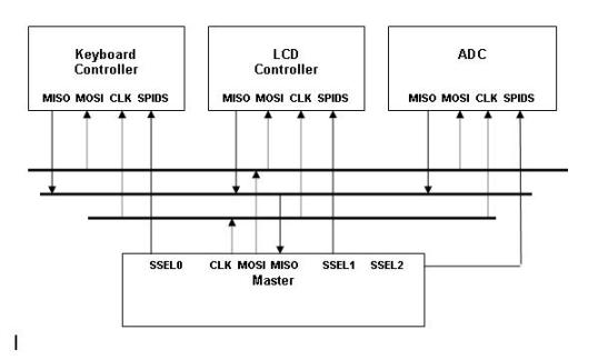
Serial Peripheral Interface (SPI) provides an easy way to communicate across various (SPI compatible) Devices in a system. SPI involves synchronous data transfers. Example of SPI compatible peripherals are Microprocessors, Data Converters and LCD Displays. Communication on SPI bus occurs with a Master and Slave relationship. Generally, a Micro-processors acts as the SPI bus master, and peripheral devices (such as Data Converters or Displays) act as slave devices. At times, there could be multiple micro-processors (or CPUs) on a given SPI bus. In such cases, a HOST processor wil act as SPI Master, and other processors will act as SPI slaves. Multi-master configurations (though rarely used) are also possible.
SPI is a four wire interface. The fours signals on SPI bus are:
* CLK : Clock signal is used for synchronizing the data transfers. It is output from Master and Input to the slave.
* MISO: stands for Master In Slave Out. As the name suggests it is output from Slave and Input to the Master. This signal is used for transferring data from Slave Device to the Master Device.
* MOSI: stands for Master Out Slave In. This signal is an output from Master and is input to the slave. It is used for transferring data from Master Device to Slave device.
* SSEL: Slave Select is output from the Master and is an input to the slave. This signal needs to be asserted (by the Master) for any transfers to be recognized by the slave. In a multi-slave configuration, Master device can have multiple slave select signals (one for each slave) and only the currently selected slave (corresponding SSEL signal asserted) will acknowledge the data transfers.
Multiple Slave Scenario
Under SPI protocol, one Master device can be connected to multiple slave devices through multiple SSEL lines. Master can assert SSEL for only the device, with who master wants to communicate. Selecting multiple slaves at a time, can damage the MISO pin (since multiple slaves will try to drive this line).
 Multi-master scenario
SPI interface provides provision for a multi-master system (at a time only one master can exist). Under such scenarios, MOSI and MISO signals need to be “Open-Drain” and these are pulled high by a resistor. This is needed to avoid the possible damage of these pins because of driver contention (multiple devices trying to drive the same signal). When a device wants to arbitrate for the bus, it polls its own SSEL line to see if there is already any master on the bus. If the bus is not free, it will wait for some time and again poll for the SSEL.
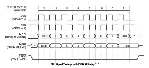
CPOL and CPHASE
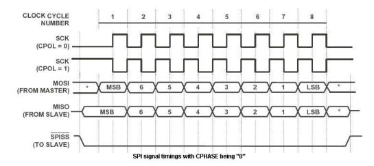
CPOL (Clock Polarity) and CPHASE (Clock Phase) settings on the SPI interface define when (on which edge of the clock) data bits are transferred (received and transmitted) across the interface. The CPOL and CPHASE configuration is very critical. Two devices communicating through SPI, should have the same settings of CPOL and CPHASE.
SPI interface is generally used used for transferring control data across devices (on the same cicuit board). Though SPI interface provides a significant improvement over UART, this interface has few drawbacks. Hardware complexity increases with increase in number of devices on the bus. Also, the multi-master scenarios are very complicated.
(c) IIC (Inter Integrated Circuit) Interface
Is a two wire interface on which multiple devices can be connected. IIC is pronounced as I-squared-C (I2C). It is a half-duplex synchronous interface. IIC was invented and promoted by Phillips, but now it is widely used by many Sillicon Vendors.
Two wire Interface: I2C consists of Clock (SCL) and Data (SDA) signals. Multiple devices can be connected on I2C bus. However at a given time, only one device (master at that instance) can drive the SCL signal. Data rates on I2C are 10kbit/s (low-speed mode), 100 kbits/s (standard mode), 400 kbits/s (Fast mode) and 3.4 Mbits/S (high Speed Mode). However intermediate data rates (which actually depends on SCL frequency) are also supported.
Addressing: Multiple devices on the I2C bus are identified by their addresses. Conventional addressing on I2C protocol is 7-bit addressing (each device on a given I2C bus will have a unique 7-bit address associated with it). Out of the total 128 possible addressing (using 7-bit addressing), 16 addresses are reserved, hence there can be maximum 112 devices on a bus. I2C protocol also supports option for 10-bit addressing (though it is rarely used).
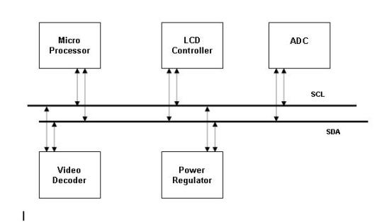
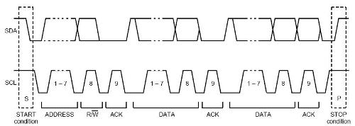
Master and Slave Relationship: When any device on the I2C bus wants to transmit or receive data, it arbitrates for the bus. After this device has obtained bus (through bus arbitration) it is called Master (since it has bus master-ship), and all other devices on the bus are called slaves. Master device initiates the data transfers and drives the clock. To initiate the data transfer, master transmits a “start bit” followed by the “address” of slave (the device with whom master wishes to communicate);, followed by a single Read/Write bit (this bit indicates if master wants to read from slave or wants to write to the slave). This is followed by data transfers (multiple of bytes). Both data and addresses are sent MSB first.
Acknowledgment: When Master device writes in to the slave (by sending single or multiple bytes of data), the slave should send an acknowledge signal after every received byte (master device waits for it before sending the next byte). In this scenario, Master releases the SDA line after transferring a byte (during the ACK clock cycle). The slave device should pull this SDA line down, to acknowledge the transfer. When master device reads data from the slave, it send an acknowledge signal to slave after reading each byte. However Master will a NO-ACK (or not send the ACK) by keeping the SDA line HIGH, after the last byte transfer. After the last byte trasfer, Master can send a START (for repeated start) OR a STOP (to end the data trasnfers and to free the bus) bit.
Bus Arbitration: A device can contend for the I2C bus (mastership) only if the bus is free (no device is currently master). If a device contends for the bus and there is not other device contending for the bus, the device will get the mastership. If two devices start contending for the mastership at (Exactly) same time, then a bus arbitration policy is used. The contending devices will monitor the state of SDA bus and compare it with the value which they are transmitting. In case a device finds that the state of the SDA bus is not same as the level which it transmitted, it will give up the bus (and again arbitrate for the bus when bus gets free). Let us say that two devices A and B wants to communicate with devices X and Y (X and Y have addresses 0×01 and 0×04 - these addresses are seven bit) respectively. A and B will transfer the addresses of X and Y on the SDA. When B is transmitting the fifth address bit (fifth from MSB), it will expect a “1″ on the address line. However in the same cycle device “A” will drive a “0″ on the bus (corresponding address bit of device Y). “0″ will pull the SDA line down, and device “B” will give up the bus.
Clock Stretching: Clock stretching is a special feature of I2C protocol, which enables the slower slave devices to signal the Master device, that it is not ready for further data transfers. The slave devices can pull down the SCL signal (clock signal) when it is not ready to receive/transmit the next data bytes from/to Master device. It is called clock stretching. When master initiates the next transfer, it also monitors the state of SCL level. If the SCL is low (at the time when master is trying to drive a High on this line), then master will delay the next transfer (as long as slave keeps the clock stretched).
(d) Synchronous SPORT
Serial PORT is mainly used for Data transfers (rather than control messages) across devices. Data transfers could be one-to-one or one-two-many. Data throughput on SPORT is generally very high as compared to other serial interfaces (like SPI and I2C). SPORT are a common peripheral on most DSPs. SPORT employ Synchronous communication with Clock and Sync Signals. Clock signal is used to synchronize each transferred bit, and Sync signal is used to synchornize each transferred word. The word size is generally programmable. Some SPORT protocols also provide an option for frame synchronization (frame consists of a number of words) rather than word synchronization. SPORT can be Duplex, Simplex or Semi-Duplex. A Duplex SPORT will have Tx, Rx, CLK and SYNC signals. CLK and SYNC can be either generated by one device on the bus (called master) or it can come from an external (external to the devices on bus) source. In this section we will use commonly used SPORT protocols.
DSP Serial mode
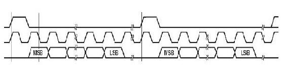
This protocol is generally employed on DSPs for bulk data tranfers. The figure below shows one of the possible configurations in DSP Serial Mode. There could be different variations to the protcol, e.g. LSB first transmission, Active Low Sync signal
I2S Serial mode
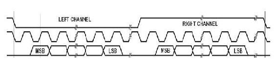
I2S mode is useful for audio data transmission. The left and right channel data is multiplexed on a single data bus, and the sync (called word clock) is used to identify the Right or Left channel. Under I2S protocol data transfers are always MSB first. Also, the first MSB is transferred in the second Clock Cycle after SYNC transition. Also, the first clock cycle may contain LSB of the last transferred word, in case the width of SYNC signal desires so (this is not shown in the figure).
Left Justified and Right Justified modes
Left Justified mode is quite similar to I2S mode. However there is a minor difference. The MSB of the word is transferred in the very first clock cycle after SYNC transition. In right justified mode, instead of aligning the MSB to first clock cycle (of current SYNC period), the LSB is aligned to the last clock cycle (of the current SYNC period).
Multi-Channel (or Time Division Multiplexed) Mode
(e) GPIOs
Are General Purpose I/O signals which can be configured either as Input or as Output. When configured as output, the state of these pins can be changed (to either “0″ or “1″) by changing the value of specific “bits” in the GPIO control registers. When configured as I/P, the physical state of these pins can be read through specific bits in the GPIO control registers.
GPIO pins can be configured as Output to send Low or High signals (this may be desired for interrupt generation, acknowledgment etc.) to any other device.
While configured as Input, the GPIO pins can be used for polling the status of a given signal. GPIOs also provide provision for an internal interrupt generation on a particular state of the GPIO pin(low or high or transition). This configuration is desired when you want to avoid the polling.
GPIOs can also be used to emulate one of the standard interfaces (like UART, SPI or I2C) using Bit-banging.
GPIOs can also be used as system status indicator. In this configuration, these pins drive certain LEDs. Based on the Low/High Level of the GPIO pin, the LED can be on (glow) or off (no glow). We will discuss such examples later in this tutorial.
(3) Parallel Peripherals
Processors provide parallel ports for data communication. Mostly these interfaces involve, N data lines, a clock line and 1 or 2 control lines (Device select, read/write etc). Timings on such interfaces are proprietary and are specific to the chip vendor. Parallel interfaces are generally useful when data throughputs are very high (can not be met with serial intrfaces).
(4) Others
USB and PCI are two very common interfaces being used for bulk data transfers. These interfaces were originally developed for PC applications and are industry standards. These intefaces are now being widely used in Embedded world.
Interrupts
We just discussed how CALL and JUMP instructions can break the linear code flow in an application. Another event which can cause the change in program flow is called "INTERRUPT". Interrupts are signals (Hardware or Software) which can cause the program sequence to stop the normal program flow and execute instructions from a certain pre-defined location (known as Interrupt Vector Address). Interrupts can be triggered by a Hardware (e.g. state of an external CPU pin) or a Software (e.g. An illegal instruction execution like divide by ZERO) event. A CPU can have multiple interrupt channels and each of these channels will have its unique interrupt vector address. When an interrupt occurs, program sequencer starts processing instructions from the Interrupt Vector Address (of the associated interrupt channel). Similar to CALL instruction, the Return Address (address of the instruction which would have been fetched in absence of an interrupt event) is saved in one of the processor registers (some CPUs also save the current system state along with return address). An RTI (Return From Interrupt) instruction (similar to RTS) can bring the program flow back to the Return Address. The code which is stored at Interrupt Vector Address is called Interrupt Service Routine (ISR). RTI instruction generally forms the last instruction of ISR.
Interrupt Controller : Is a Hardware inside the Processor which is responsible for managing the interrupt operations.
Enabling Interrupts : Interrupts (on most processors) can be enabled or disabled by the programmer using a (Global) Interrupt Enable Bit. Interrupt Controllers also provide option for enabling or disabling each individual interrupt (on a local level).
Interrupt Masking : Interrupt Mask is a control word (generally stored in a Interrupt Mask Register) which can be used to temporarily disable an interrupt (on a particular channel). The Interrupt Mask contains control bits (mask bits) for each interrupt channel. If this bit is set, the interrupt for the corresponding interrupt channel is temporarily masked (and it remains masked unless the mask bit is cleared).
Interrupt Priority : Interrupt Channels are associated with different priority levels. If two interrupts are acknowledged by the Interrupt Controller at same time, then the higher priority interrupt is processed first. Interrupt Priority Scheme helps to ensure that more important (interrupt) events gets processed first (as compared to less critical events. Critical Events (e.g. system power failure) are assigned with highest priority.
Interrupt Mapping : Some Interrupt Controllers also provide flexibility of mapping the interrupt sources (events that generate events) to any of the available interrupt channel. This scheme has two major advantages. Firstly, in a system, (generally) not all the interrupts sources are active at a time. A fixed mapping (from source to channel) means that many of the interrupt channels will be un-utilized. However with a flexible mapping, it is possible to provide lesser interrupt channels (and active sources can be mapped to these channels). This reduces the Hardware complexity of Interrupt controller, and hence cost. Interrupt controller can also provide provision for mapping multiple sources to a single interrupt channel. In the ISR (for particular interrupt), the interrupt source (out of many sources mapped to this channel) can be identified by reading interrupt status register (this register has the corresponding bit set if an interrupt event occurs). Secondly, the interrupt sources can be assigned to interrupt channels with different priorities, based on the system requirement.
DMA
DMA (Direct Memory Access) provides an efficient way of Data Transfers across "a Peipheral and Memory" or across "two memory regions". DMA is a processing engine which can perform data transfer operations (to or from the Memory). In absence of DMA engine, the CPU needs to handle these data operations, and hence the overall system performance is heavily reduced. DMA is specifically useful in the system which involve huge data transfers (in absence of DMA, CPU will be busy doing these transfers most of the time and will not be available for other processing).
DMA Parameters : DMA Transfers involve a Source and a Destination. DMA Engine Transfers the data from Source to Destination. DMA engine requires source and destination addresses along with the Transfer Count in order to perform the data transfers. The (Source or Destination) Address could be a physical address (in case of a memory) or logical (in case of a peripheral). Transfer Counts specifies number of words which need to be transferred. As we mentioned before, Data transfer could be either from a Peripheral to Memory (generall called Received DMA) or from a Memory to Peripheral (generally called Transmit DMA) or from a Memory to another Memory (Generally called Memory DMA).
Some DMA engines support additional parameters like Word-Size, and Address-Increment in addition to the Start Address and Transfer Count. Word-Size specify the size of each transfer. Address-increment specifies the offset from current address (in memory), which the next transfer should use. This provides a way of tranferring data from non-contiguous memory locations.
DMA Channels : DMA engine can support multiple DMA Channels. This means that at a given time, multiple DMA Transfers can happen (though physcially only one transfer may be possible, but logically DMA can handle many channels in parallel). This feature makes the life of software programmer very easy (as he does not have to wait for the current DMA operations to finish before he programs the next DMA operation). Each DMA channel will have control register where the DMA Parameters can be specified. DMA Channels also have an interrupt associated with it (on most processors) which (optionally) triggers after completion of DMA trasfer. Inside the ISR, programmer can take specific action (e.g. do some processign on the data which has been just received through DMA, or program a new DMA transfer).
Chained DMA : Certain DMA controllers support an option for specifying DMA parameters in a Buffer (or array) in memory rather than directly writing it to DMA control registers (This is mostly applicable for the second DMA operation - parameters for first DMA operation are still specified in the control registers). This Buffer is called DMA Transfer Control Block (TCB). DMA controller takes the address of DMA TCB as one of the parameters, (in addition to the control parameters for first DMA transfer) and loads the DMA parameters (for second DMA operation) automatically from the Memory (after first DMA Operation is over). The TCB also contains an entry for "Next TCB Address", which provides an easy way for chaining multiple DMA operations in an automatic fashion (rather than having to program it after completion of each DMA). The DMA chaining can be stopped, by specifying a ZERO address in Next TCB Address field.
Multi-diemnsional DMA : combined with Address-Increment gives many options.
User Comments
No Posts found !Login to Post a Comment.