Ports
Term "port" refers to a group of pins on a microcontroller which can be accessed simultaneously, or on which we can set the desired combination of zeros and ones, or read from them an existing status. Physically, port is a register inside a microcontroller which is connected by wires to the pins of a microcontroller. Ports represent physical connection of Central Processing Unit with an outside world. Microcontroller uses them in order to monitor or control other components or devices. Due to functionality, some pins have twofold roles like PA4/TOCKI for instance, which is in the same time the fourth bit of port A and an external input for free-run counter. Selection of one of these two pin functions is done in one of the configuration registers. An illustration of this is the fifth bit T0CS in OPTION register. By selecting one of the functions the other one is disabled.
All port pins can be designated as input or output, according to the needs of a device that's being developed. In order to define a pin as input or output pin, the right combination of zeros and ones must be written in TRIS register. If
the appropriate bit of TRIS register contains logical "1", then that pin is an input pin, and if the opposite is true, it's an output pin. Every port has its proper TRIS register. Thus, port A has TRISA, and port B has TRISB.
Pin direction can be changed during the course of work which is
particularly fitting for one-line communication where data flow constantly
changes direction. PORTA and PORTB state registers are located in bank 0,
while TRISA and TRISB pin direction registers are located in bank 1.
PORTB and TRISB
PORTB has adjoined 8 pins. The appropriate register for data direction is TRISB. Setting a bit in TRISB register defines the corresponding port pin as input, and resetting a bit in TRISB register defines the corresponding port pin as output.
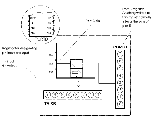
Each PORTB pin has a weak internal pull-up resistor (resistor which defines a line to logic one) which can be activated by resetting the seventh bit RBPU in OPTION register. These 'pull-up' resistors are automatically being turned off when port pin is configured as an output. When a microcontroller is started, pull-ups are disabled.
Four pins PORTB, RB7:RB4 can cause an interrupt which occurs when their status changes from logical one into logical zero and
opposite. Only pins configured as input can cause this interrupt to occur (if any RB7:RB4 pin is configured as an output, an interrupt won't be generated at the change of status.) This interrupt option along with internal pull-up resistors makes it easier to solve common problems we find in practice like for instance that of matrix keyboard. If rows on the keyboard are connected to these pins, each push on a key will then cause an interrupt. A microcontroller will determine which key is at hand while processing an interrupt It is not recommended to refer to port B at the same time that interrupt is being processed.
| bsf | STATUS, RP0 | ;Bank1 |
| movlw | 0x0F | ;Defining input and output pins |
| movwf | TRISB | ;Writing to TRISB register |
| bcf | STATUS, RP0 | ;Bank0 |
| bsf | PORTB, 4 | ;PORTB <7:4>=0 |
| bsf | PORTB, 5 | |
| bsf | PORTB, 6 | |
| bsf | PORTB, 7 |
The above example shows how pins 0, 1, 2, and 3 are designated input, and pins 4, 5, 6, and 7 for output,
after which PORTB output pins are set to one.
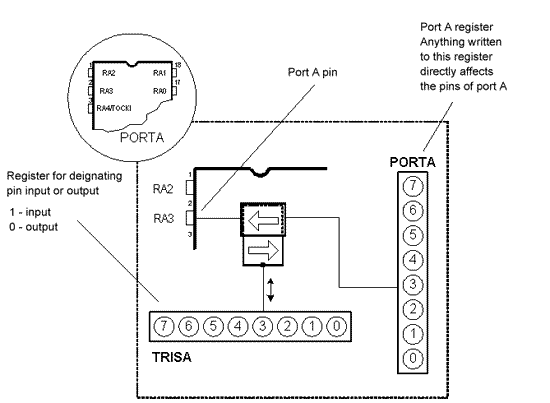
PORTA and TRISA
PORTA has 5 adjoining pins. The corresponding register for data direction is TRISA at address 85h. Like with port B, setting a bit in TRISA register defines also the corresponding port pin as input, and clearing a bit in TRISA register defines the corresponding port pin as output.
It is important to note that PORTA pin RA4 can be input only. On that pin is also situated an external input for timer TMR0. Whether RA4 will be a standard input or an input for a counter depends on T0CS bit (TMR0 Clock Source Select bit). This pin enables the timer TMR0 to increment either from internal oscillator or via external impulses on RA4/T0CKI pin.
|
|
RA4 pin can be designated output, but in that case it has to be externally connected to PULL-UP resistor. |
Configuring port A:
| bsf | STATUS, RP0 | ;Bank1 |
| movlw | b'11111100' | ;Defining input and output pins |
| movwf | TRISA | ;Writing to TRISA register |
| bcf | STATUS, RP0 | ;Bank0 |
Example shows how pins 0, 1, 2, 3, and 4 are designated input, and pins 5, 6, and 7 output. After this, it is possible to read the pins RA2, RA3, RA4, and to set logical zero or one to pins RA0 and RA1.
User Comments
No Posts found !Login to Post a Comment.